13
submitted 1 year ago by PaX@hexbear.net to c/technology@hexbear.net

cross-posted from: https://hexbear.net/post/621898

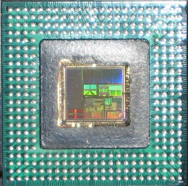
In this photo, you can see how much the on-die cache has expanded compared to its predecessors and other contemporary embedded microprocessors. Really foreshadowing the kind of optimizations that would become commonplace today. In addition to its very large (for the time) 4-way set associative 256kb on-die secondary cache, it featured a 16k primary instruction cache and 16k primary data cache. It was fabricated at a 250 nanometer feature size and could be clocked up to 263 MHz. With its dual-issue superscalar 5-stage pipeline, it could achieve a Dhrystone score of 450 DMIPS at 263 MHz, a impressive score for embedded microprocessors of the time, although this benchmark really doesn't show off its cache performance.

Anyway, hope you like the pretty die shot of this forgotten microprocessor.
top 3 comments
sorted by: hot top controversial new old
[-] RNAi@hexbear.net 3 points 1 year ago
[-] PaX@hexbear.net 3 points 1 year ago

It's a picture of the inside of a computer processor.

Here's a zoomed out version for scale:

[-] WilsonWilson@hexbear.net 2 points 1 year ago

If you want to learn more about cpu design I would recommend Ken Shirriff's blog. He reverse engineers OG CPUs and explains how everything works. He's well known among electrical engineering spaces for doing this as well as breaking down a SHA-256 calculation with pencil and paper.

this post was submitted on 17 Sep 2023
13 points (100.0% liked)

technology

23313 readers
243 users here now

On the road to fully automated luxury gay space communism.

Spreading Linux propaganda since 2020

Rules:

founded 4 years ago
MODERATORS