view the rest of the comments
Ask Science
Ask a science question, get a science answer.
Community Rules
Rule 1: Be respectful and inclusive.
Treat others with respect, and maintain a positive atmosphere.
Rule 2: No harassment, hate speech, bigotry, or trolling.
Avoid any form of harassment, hate speech, bigotry, or offensive behavior.
Rule 3: Engage in constructive discussions.
Contribute to meaningful and constructive discussions that enhance scientific understanding.
Rule 4: No AI-generated answers.
Strictly prohibit the use of AI-generated answers. Providing answers generated by AI systems is not allowed and may result in a ban.
Rule 5: Follow guidelines and moderators' instructions.
Adhere to community guidelines and comply with instructions given by moderators.
Rule 6: Use appropriate language and tone.
Communicate using suitable language and maintain a professional and respectful tone.
Rule 7: Report violations.
Report any violations of the community rules to the moderators for appropriate action.
Rule 8: Foster a continuous learning environment.
Encourage a continuous learning environment where members can share knowledge and engage in scientific discussions.
Rule 9: Source required for answers.
Provide credible sources for answers. Failure to include a source may result in the removal of the answer to ensure information reliability.
By adhering to these rules, we create a welcoming and informative environment where science-related questions receive accurate and credible answers. Thank you for your cooperation in making the Ask Science community a valuable resource for scientific knowledge.
We retain the discretion to modify the rules as we deem necessary.

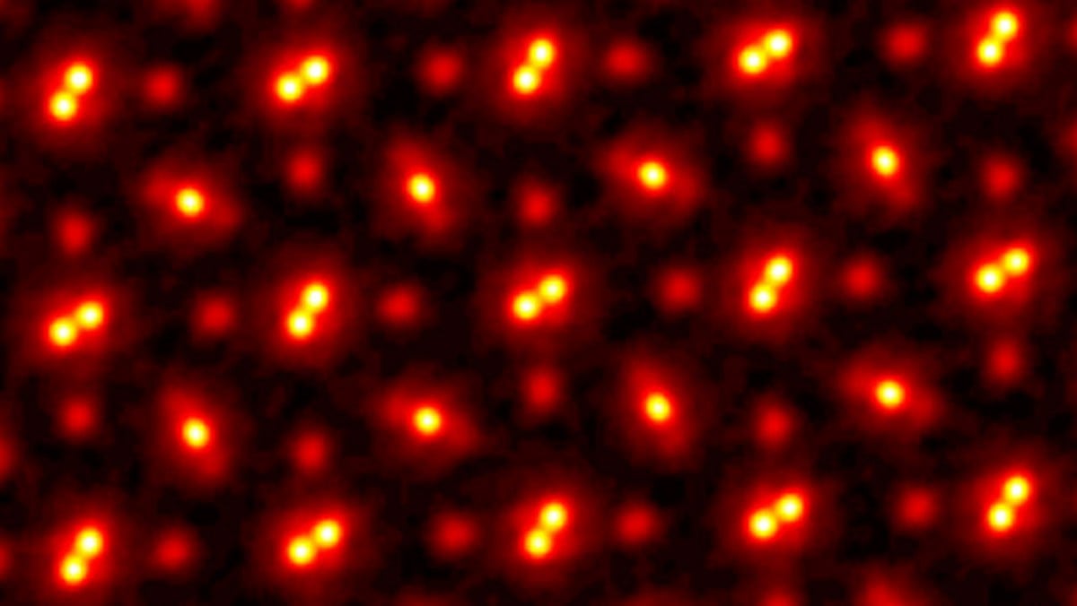
That is only sort of true - this image is not made of electrons reflected by the nuclei. These are results from TEM imaging, so Transmission Electron Microscopy. The electron detector is placed behind the sample.
What you are describing is SEM - Scanning Electron Microscopy - in that case, the detector can be placed above the sample, for example (but not limited to) circularly around the beam to measure the backscattered electrons
In TEM the samples are cut into very thin slices (in the picture you posted it is said to be between 0.8nm - 30nm) and the crystal lattice acts as a diffraction grating for the electron beam. The diffraction pattern can be then used to reconstruct the crystal lattice structure.